preload-image

Product

Our products

blog post image

Silicon wafer 1-12inch

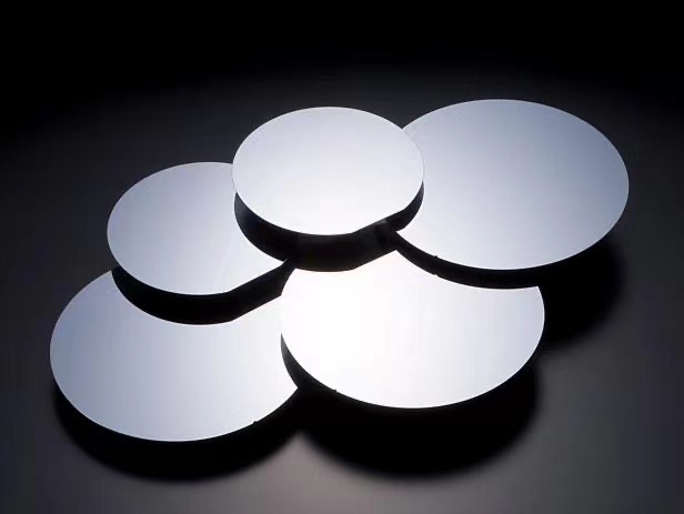
Silicon Ingot and Wafer N or P Tpye; Orien.<100>、<111>、<110> Res.0.001-100ohm; 30-5000ohm; Intrinsic FZ 300-10000ohm Ingot Length: 150mm-350mm; Dia.: 2inch~8inch; Wafer Dia.: 2inch~12inch;Thick.:SEMI Standard or as per customers’ Spec. Dislocation/Slip/Crack/Chip/Pin Hole/Broken:Free

blog post image

SiC wafer 2-8 inch

Silicon carbide (SiC) was discovered in 1893 as an industrial abrasive for grinding wheels and automotive brakes. About midway through the 20th century, SiC wafer uses grew to include in LED technology. EST offers prime and dummy SiC wafers in a variety of diameters ranging from 2” to 8” (200mm).

blog post image

GaN wafer 2-6inch

Free standing GaN (Gallium Nitride) substrate wafer is mainly used for UHB-LED and LD application. The well-known effect of using free-standing GaN substrates can be improved material quality, reducing parasitic resistance effects for creating nitride semiconductor devices.

blog post image

LT/LN wafer 3-6inch

The basic principle of SAW devices is the generation of elastic surface waves from electrical signals and their reconversion. The substrate material is a piezoelectric crystal such quartz (SiO2), lithium tantalate (LiTaO3) or lithium niobate (LiNbO3).

blog post image

Sapphire wafer 2-8 inch

EST provides 2", 4" and 8 " C-plane, R-plane sapphire wafers. SSP or DSP. Standard thickness at 1200um, 650um and 430um, thin wafers are available, and other specific specifications can provide upon your request.

Newsleter

Back-To-Top